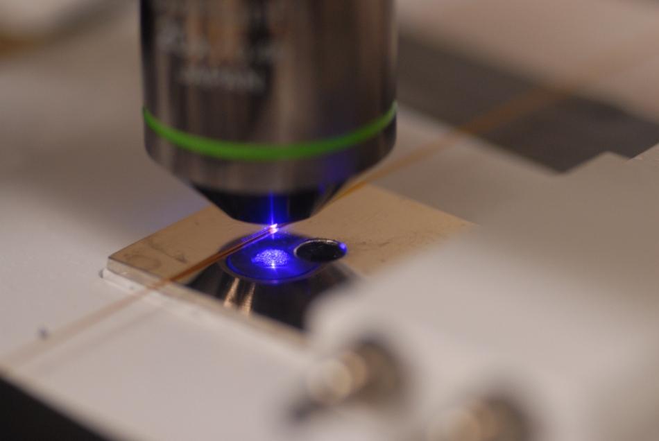
During my research, I worked at the crossroads of physics, microelectronics, biology and chemistry to develop miniaturized laboratories based on PNIPAM, a polymer that changes properties with temperature.
Using techniques developed for microelectronics, researchers are able to miniaturize entire lab functions to the size of a microchip, paving the way for cheap, reliable testing kits and biomedical devices that fit in your pocket. However, shrinking a whole lab onto a chip changes the balance of physical forces, and how liquids behave at the microscale.
Overview

I studied how to use PNIPAM to control the flow of fluids in micro channels, and to trap and release proteins for biological analysis. I conducted this research with Anne-Marie Gué and Jan Sudor at the Laboratory for Analysis and Architecture of Systems (LAAS-CNRS) in Toulouse, France.
Technical abstract
Labs-on-a-chip are miniaturized devices integrating one or several laboratory functions, usually dedicated to the handling of chemical and biological samples. My work aimed at integrating a smart polymer called poly(N-isopropylacrylamide) (PNIPAM) in microsystems, in order to develop a new technological process for labs-on-a-chip.
PNIPAM is a thermosensitive polymer that undergoes a reversible state transition; it switches from a hydrophilic, swollen state below its temperature of transition (LCST ~ 32°C), to a hydrophobic, collapsed state above it. The technology I developed was based on heating elements and a surface functionalization process to graft the PNIPAM layer.
My results showed that the electro-osmotic flow could be modulated by thermally controlling the PNIPAM, thus paving the way for electrokinetic mixers. This thermal control also enabled the adsorption (and partial desorption) of proteins on fonctionalized beads, the main application being sample preparation.
Honey, I shrunk the lab.
.jpg)
G.Cooksey, NIST on Wikimedia Commons // Public domain.
Using techniques developed for microelectronics, researchers are able to miniaturize entire lab functions to the size of a microchip, paving the way for cheap, reliable testing kits and biomedical devices that fit in your pocket.
At-home pregnancy tests are some of the simplest examples of miniaturized devices for biological analysis. They take in a direct sample (urine) that doesn’t require further preparation, and detect a molecule of interest in it (the human pregnancy hormone, hCG). Similarly, diabetic people use glucose meters with test strips to measure the glucose levels in their blood. The Covid-19 pandemic has also introduced many people to the need for rapid, cheap testing and diagnosis. At-home Covid tests are very similar to pregnancy tests, if slightly more involved: the sample must usually be collected with a dry swab, and then diluted into a liquid for analysis on a strip.
All these tests are relatively inexpensive and widely available; they provide a generally reliable result within minutes and don’t require specialized technical expertise. They don’t necessarily replace further professional analysis in a full-fledged lab, but they provide quick results by bringing the lab to you in small package. They are the very basic (and rather large) cousins of labs-on-a-chip.
Technically, pregnancy tests may even qualify as the simplest example of micro total analysis systems (microTAS), a class of miniaturized systems that integrate the complete sequence of analysis from a raw sample (saliva, urine, blood) up to the test result. Labs-on-a-chip don’t always accept raw samples, and may include only specific functions of the sequence of analysis, because integrating the whole chain isn’t possible or beneficial.
Advanced labs-on-a-chips integrate several lab functions into a miniaturized device. They combine the advances made in consumer electronics through the very large scale integration of transistors, with applications in biology and medicine. As such, they build on the expertise, tools, and processes in semiconductor manufacturing, to design and mass-produce reliable testing units at low cost.
Miniaturization has advantages inherent to biological analysis as well. By integrating multiple lab functions close together on a single chip, labs-on-a-chip require much smaller volumes of samples and chemical substances. Connections are simplified and sample waste is reduced. Disposable, single-use chips also limit cross-contamination.
Labs-on-a-chip can lead to performance improvements in separation analysis like capillary electrophoresis, where miniaturized channels decrease molecular and thermal diffusion distances. Combining biological analysis and electronics into single devices also opens the door to dramatic improvements in automated analysis and high-throughput screening. This becomes particularly relevant to address new challenges of molecular biology in fields such as transcriptomics, proteomics, metabolomics, cellomics, and other -omics sciences.
Test kits integrated on a chip are often portable and usable by people with limited expertise. Large batches of units may be shipped during a large-scale health crisis, and support clinical diagnosis as close to the patient as possible, in particular in geographies and contexts that lack full-fledged bioanalysis labs. Other applications of labs-on-a-chip include environmental monitoring (e.g. testing for contaminants in food and water), pharmaceutical research (high-throughput screening for drug discovery) and defense against bioterrorism.
Microfluidics

In nature, the capillary action inside the tiny veins of a plant manages to overcome the force of gravity to draw water upwards to its leaves. Similarly, shrinking a whole lab onto a chip changes the balance of physical forces, and how liquids behave at the microscale.
At the macroscale of humans, water obeys the laws of gravity and goes down, as anyone who has spilled their tea can attest. But at the microscale, water and other fluids behave differently, bringing us into the world of microfluidics.
Physical phenomena don’t decrease linearly (or homothetically) as dimensions shrink; some effects, like capillarity, friction, and electrical forces, start to overtake usual driving forces like gravity. It’s why small insects, lizards, and spiders can walk up walls and ceilings, but would have a much harder time doing so if they were enlarged to the size of a cat.
Miniaturization dramatically increases the surface-to-volume ratio, meaning that surfaces take a stronger role: for example, molecules stick to walls, and liquids evaporate, especially droplets. Building microfluidic systems calls for precise control of physical and chemical phenomena happening on surfaces, which can be done through surface functionalization.
Developing miniature labs therefore requires a whole microplumber’s toolbox to move liquids around, like microchannels, pumps, valves, and mixers. The interface with the human world involves connecting two systems of very different scales, akin to picking up a single strand of hair off the floor using your fingers.
More complex microfluidic functions include magnetic or optical elements coming from the field of micro-electromechanical systems (MEMS). Technological bricks developed to assemble labs-on-a-chip include sample preparation and preconcentration, microreactors, chemical separation by chromatography and electrophoresis, and detection through fluorescence and mass spectrometry.
PNIPAM
There are many ways to control the behavior of surfaces in microfluidic systems. My research focused on PNIPAM, a special kind of polymer whose properties change with temperature.
Polymers are macromolecules (very large molecules) composed of a bunch of smaller identical molecules called monomers. Imagine overcooking spaghetti to the point where all the individual strands start to stick together and form a larger (unappetizing) blob, and you’ll get a pretty good idea of how polymers are formed. The physical properties of some polymers change when something in their environment varies (pH, temperature, ionic strength, electric field, light, etc.); PNIPAM is such a stimuli-responsive polymer.
The simplest way to describe PNIPAM is as a goey substance that changes when it gets hot. At room temperature, it likes to spread in water: it’s hydrophilic. But if you heat it to around 32°C (90°F), it doesn’t like water any more: it becomes hydrophobic. It shrinks onto itself so it can be the least wet possible. If you lower the temperature again, it reverts to being hydrophilic, unfolds, and spreads its arms in water.
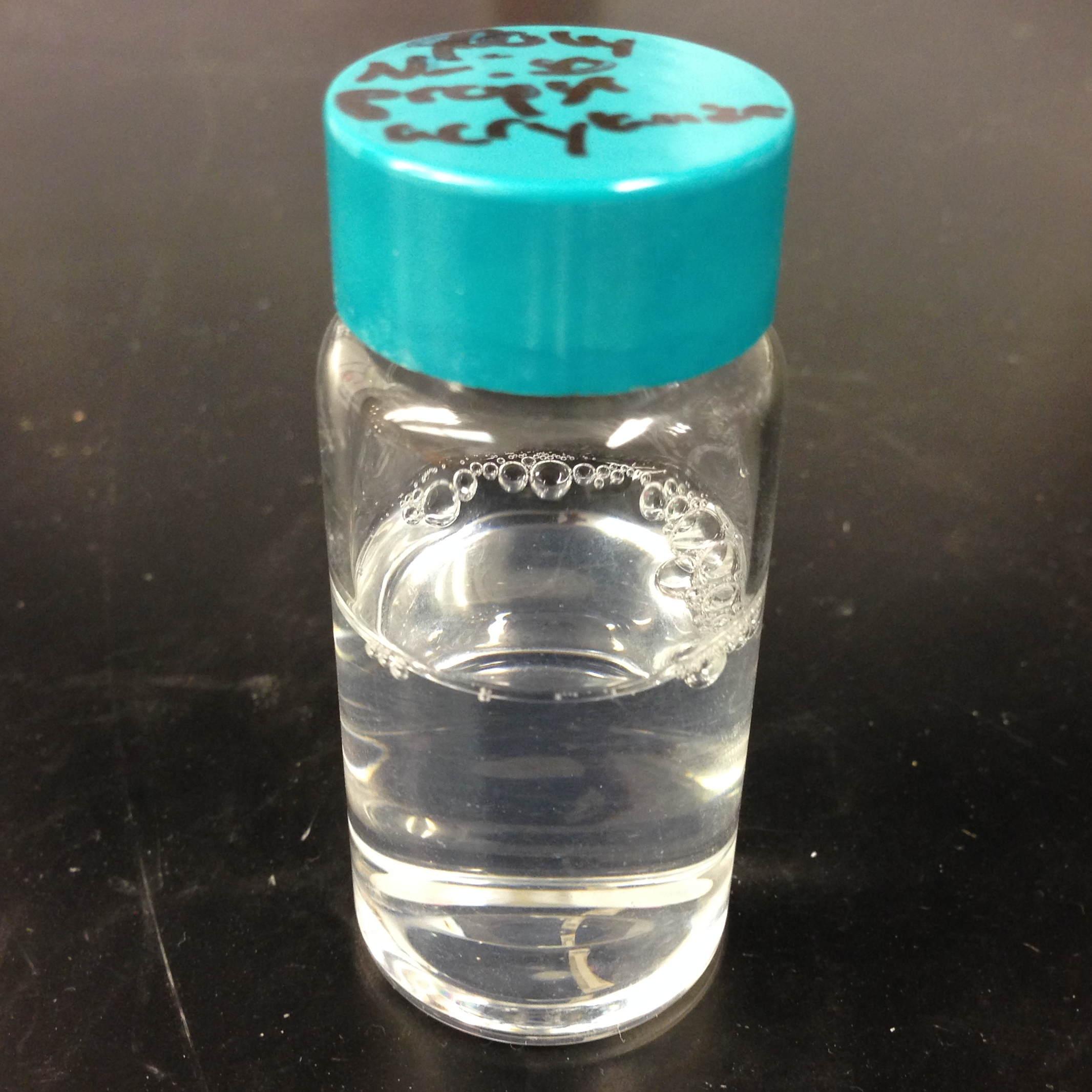
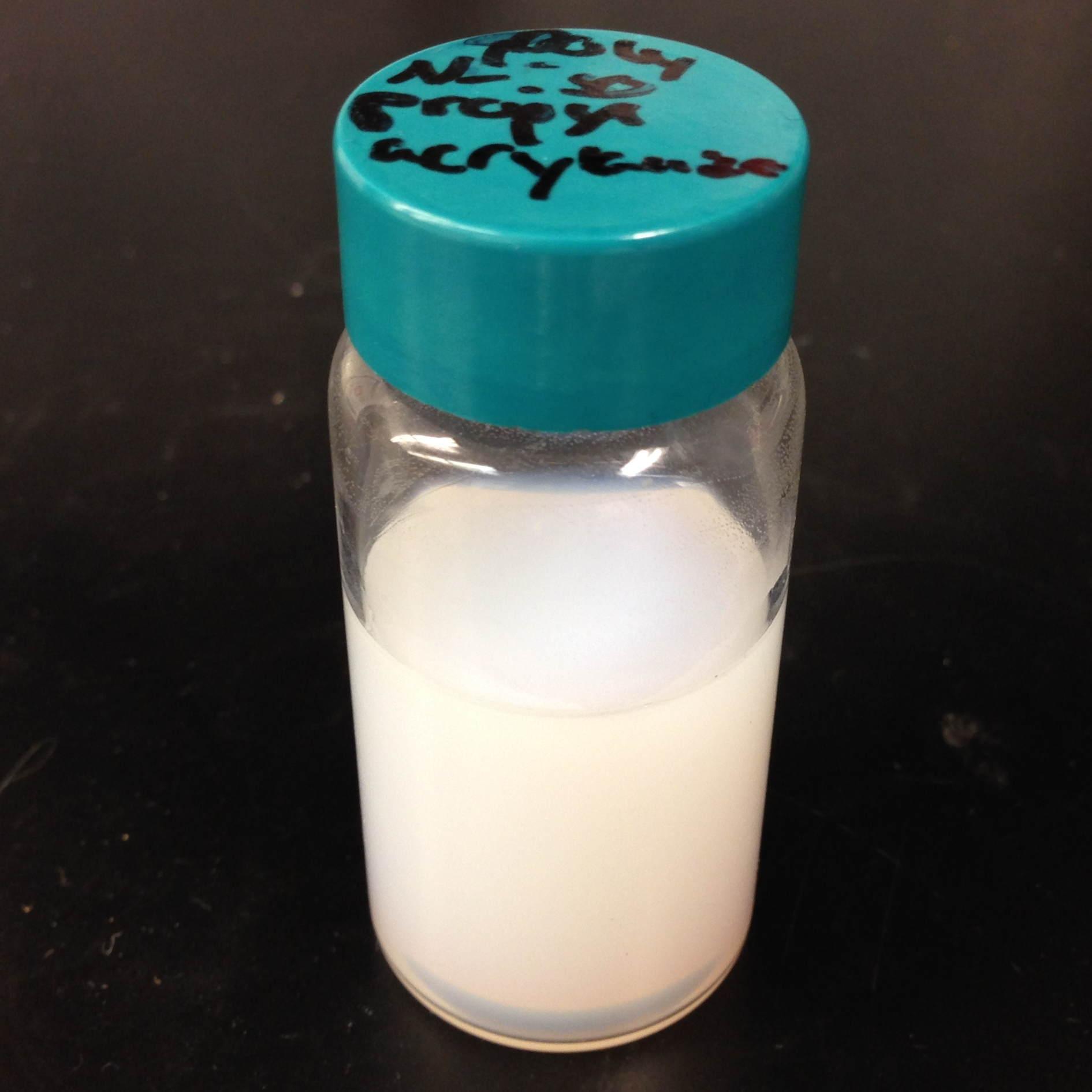

At room temperature (left), a solution of PNIPAM is transparent because the polymer is dissolved in water. When heated above 32°C (right), the solution becomes opaque as the polymer shrinks. Rg is the radius of gyration, used to describe the dimensions of the polymer chains. (Top: Quantyield on Wikimedia Commons: 1, 2 // CC BY-SA 3.0)
In technical terms, poly(N-isopropylacrylamide) (CAS: 25189-55-3) is a thermosensitive polymer that undergoes a reversible coil-to-globule conformational transition from a hydrophilic, swollen state to a hydrophobic, collapsed state around 32°C. Above its lower critical solution temperature (LCST), it becomes insoluble in water, turning opaque and sterically hindered.
While there are some uses for PNIPAM in liquid solutions, it often needs to be grafted to a surface. Attaching chemical molecules to a surface is a broad field of chemistry known as surface functionalization.
Surface functionalization

Attaching PNIPAM to a surface involves successive chemical steps, like applying coats of primer, paint, and finish onto a wall, each layer building on the previous one. In the end, PNIPAM looks like a layer of microscopic moss.
Grafting chemistry
To attach PNIPAM on surfaces, chemists use a primer layer of silane. Silanes are molecules that include an atom of silicon, which makes them useful to attach all sorts of other molecules on surfaces made of silicon, silicon oxide, and glass (an amorphous kind of silicon oxide). Silicon and silicon oxides are omnipresent in microelectronics and its micro-engineering processes, many of which are now used to make microsystems and labs-on-a chip. The specific “silanization” protocol I used to attach PNIPAM was one with which I had worked extensively during my time at CEA-Léti to graft antibodies, peptides, and enzymes to silicon surfaces.
I used 3-(Trimethoxysilyl)propyl methacrylate (TMSPM, CAS: 2530-85-0) as a preliminary silane layer. Its trimethoxysilane end attaches to silicon and silica surfaces, such as silicon wafers (with native oxide or thermal oxidation), glass slides, PECVD oxide layers, and silica beads.
The silanization process, called “CEA-2,” was developed at the CEA-Léti lab to attach biological probes on biochips. It results in a covalent —Si—O—Si— bond between the surface and the silane.
The methacrylate end of TMSPM serves as starting point for the radical chain polymerization of PNIPAM and polyacrylamide, the latter of which I used as a temperature-insensitive control for PNIPAM in some experiments.
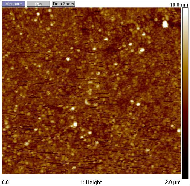
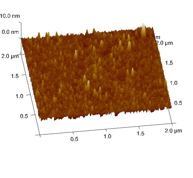
Silica surface coated with TMSPM after silanization, observed by atomic force microscopy.
Contact angle
Testing the wettability of the surface is an easy way to verify the steps of the silanization and polymerization processes. Water behaves differently on the the surface of various materials. For example, clean metal surfaces are hydrophilic, meaning they attract water: droplets spread out on them and have a very flat profile, making a small angle with the surface.
Many plants, in contrast, have hydrophobic leaves: they repel water; droplets stick out higher, in a more rounded shape. Ultrahydrophobic surfaces can display self-cleaning properties like the Lotus effect, and have inspired man-made water-repellent coatings, paints, and fabrics. At room temperature, PNIPAM is hydrophilic, like clean metal, and when heated it becomes hydrophobic, like plant leaves, and the angle of the droplet is much higher.


Left: Flat water droplets on a hydrophobic metallic surface (Olia Gozha on Unsplash). Right: Round water droplet on a hydrophobic plant leaf (Lukas Bato on Unsplash).
In technical terms, I conducted contact angle measurement by sessile drop to check the successive steps of the surface functionalization. To characterize PNIPAM surfaces, I conducted dynamic contact angle measurements, showing that the advancing angle on a PNIPAM surface increases with temperature, as the surface turns hydrophobic.
I also studied the contact angle hysteresis on PNIPAM over temperature, which followed the advancing angle pattern. My colleagues in atomic scale modeling offered an explanation based on the presence of syndiotactic NIPAM monomers in PNIPAM chains, whose polar amide groups wouldn’t be saturated by intramolecular interactions in the collapsed state as in the isotactic form, and would be free to interact with water molecules in the solution.
Infrared spectroscopy
Measuring the angle of a droplet of water is limited in the amount of information it provides. More advanced (but heavier) characterization methods can determine the chemical composition of the molecules present on the surface.
Using Attenuated total reflectance infrared spectroscopy (ATR-IR) and Fourier-transform infrared spectroscopy (FTIR), our colleagues were able to confirm the presence of chemisorbed PNIPAM and its grafting silane layer.
Controlling surface properties with PNIPAM

In microscopic channels, liquids move in a very smooth, parallel fashion, like the Aletsch glacier in the Alps. One way to create turbulence to mix liquids is to change the electrical properties of the surface. I conducted experiments to measure the flow of liquids in microchannels coated with PNIPAM, and activated it with temperature to control the flow.
Electrokinetic mixing
When liquids have enough room to move around, mixing them is relatively easy; but when they’re trapped in a small tube, they’re much more constrained, and can’t mix as freely: not much mixing happens in a straw, for example.
In microfluidics, this behavior is referred to as laminar flows. In order to miniaturize lab tools and create labs-on-a-chip, new ways to mix liquids are needed. Active micromixers rely on an external power source to generate turbulence, for example through electrokinetic, magnetic, or acoustic effects. Passive mixers require no external energy and instead solely rely on the geometry or microstructures of the channel.
It is possible to design an active electrokinetic micromixer based on PNIPAM by using it to control electrical phenomena at the local liquid-solid interface in microchannels. In other words, miniaturized heating elements create a checkerboard of PNIPAM and electrical charges on the surface, which creates turbulence.
In technical terms, systems with a low Reynolds number result in laminar flows, in which mixing only happens through diffusion. Electrokinetic mixers based on PNIPAM rely on electro-osmosis, i.e. the bulk movement of an electrolyte across a conduit with a charged surface under the application of an electrical potential. Heterogeneous charges on the surface can lead to recirculation of the liquid, creating convective rolls and acting as mixers.

In a PNIPAM-based electrokinetic mixer, miniaturized, addressable heating elements enable microscopic control of the state of PNIPAM, which creates patterns of surface charges leading to convective rolls and recirculation.
Electro-osmotic flow
Electro-osmosis happens when a liquid that contains electrical charges is in a conduit like a capillary or a membrane. When you apply an electrical potential across that conduit, the liquid moves. The resulting electro-osmotic flow depends on the electrical charges on the surface, for example on the interior wall of a capillary tube.
The electrical double layer is a model that describes the electrical potential in an electrolyte near a surface. A first, dense layer of counter-ions (Stern layer ≤ 1 nm) mirrors the opposite surface charges, while a second, diffuse layer (Gouy-Chapman layer ∼10 nm) screens the first layer from the rest of the otherwise neutral liquid. The ζ-potential, defined as the potential difference between the Stern layer and the liquid, is characteristic of the electrical charges on the surface.
A common way to reduce electro-osmosis is to attach a polymer on the surface, thus hiding the electrical charges, and locally modifying the liquid’s surface viscosity. In its swollen state, PNIPAM can serve this purpose, while in its collapsed state it exposes the electrical charges once again and the electro-osmotic flow resumes. In other words, PNIPAM enables us to hide and show surfaces charges on command by changing its temperature.
Controlling the electro-osmotic flow with PNIPAM
To create electrokinetic mixers, I needed to prove that PNIPAM could respond to temperature and change the electrical charges inside tiny channels. I therefore measured the impact of PNIPAM on the motion of a liquid under an electrical potential.

I measured the electro-osmotic flow in a capillary C whose interior wall was coated with PNIPAM. Two reservoirs 1 and 2 contain slightly different concentrations of a Tris/Borate/EDTA buffer (TBE). As the liquid inside the capillary is replaced due to the electro-osmotic flow, the resistivity of the electrical circuit changes, and so does the electrical current. The temperature was controlled by placing the setup in a laboratory oven.
The electro-osmotic mobility µ can be measured by observing the electro-osmotic flow using current monitoring between two buffer solutions of slightly different concentrations, joined by a capillary. After repeating the experiment dozens of times through a range of temperatures, the electro-osmotic mobility can be plotted as a temperature study (below). The results show that the electro-osmotic mobility follows the transition of PNIPAM around 32°C and varies by an order of magnitude between the two states.

This chart shows the typical, fast electro-osmotic flow measured in an uncoated capillary; after 40 seconds, the liquid inside the capillary was completely replaced and the current reached a plateau (6 experiments overlaid for reproducibility). The electro-osmotic mobility µ is derived from this data.
The temperature study of the electro-osmotic flow in microchannels coated with PNIPAM validated the principle of electrokinetic mixers based on the thermosensitive polymer. One of my colleagues then led the development of miniature heating elements to create addressable patterns of charges on the surface.

A temperature study of the electro-osmotic mobility in a capillary coated with PNIPAM shows a the effect of PNIPAM around 32°C (146 experiments, electrical field 400 V/cm, TBE buffers 0,5× and 0,45×).
Microfluidic chip
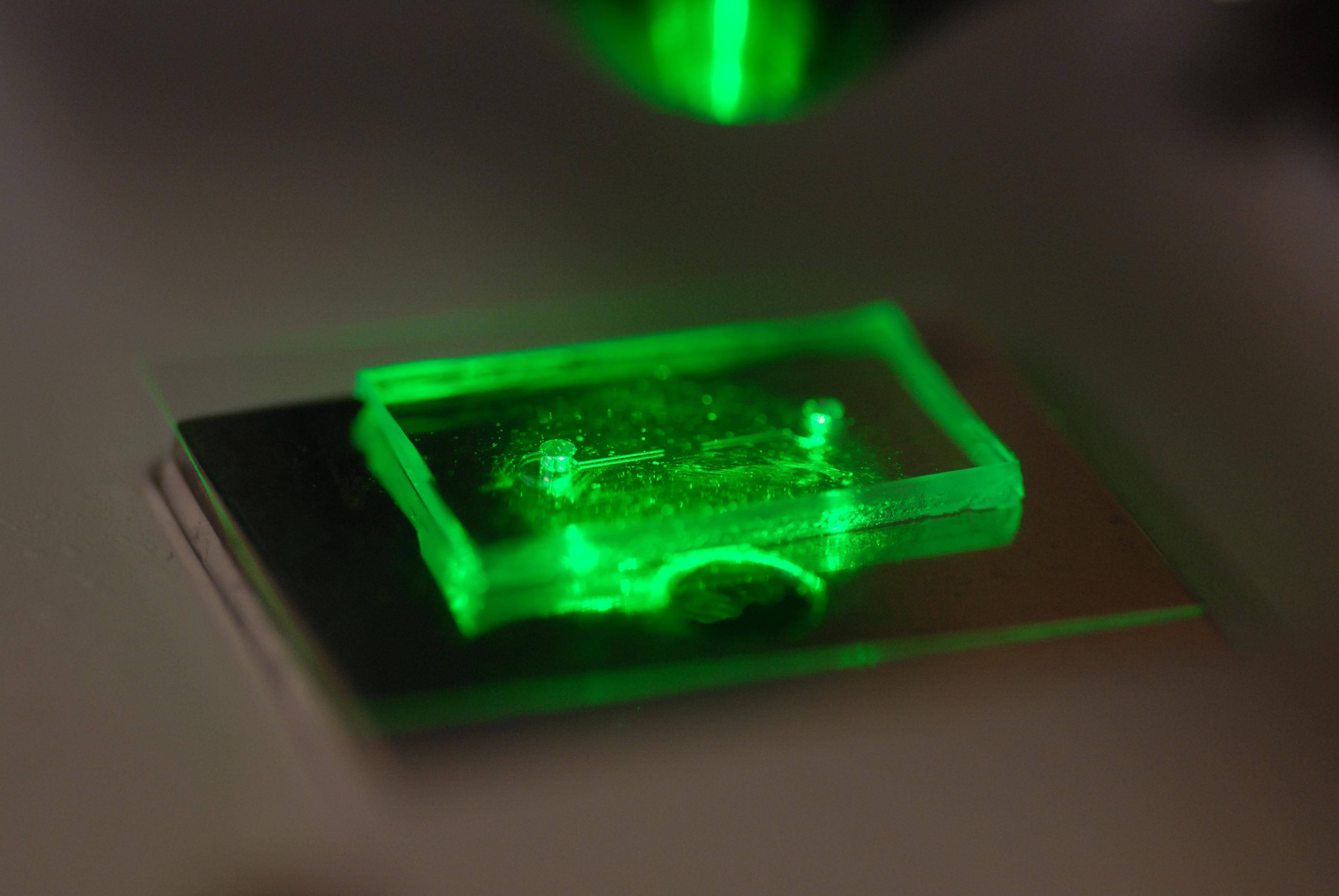
Another application of PNIPAM is the trapping and release of proteins in labs-on-a-chip. I developed and built a microfluidic chip using techniques from microelectronics and materials adapted to biological applications.
Due to the legacy of semiconductors and microelectronics, microfluidics and labs-on-a-chip have inherited the techniques, processes, and machines that have brought about the transistor and the Information Age. As a silicon oxide, glass is compatible with many of the fabrication chains that have historically handled silicon wafers. Some biological applications, like electrophoresis, involve high voltages, for which glass is better suited due to its insulating properties. Its transparency is also attractive for microscopy and detection by fluorescence.
Polymers have become a material of choice for labs-on-a-chip as well. In particular, PDMS (polydimethylsiloxane, CAS: 63148-62-9) is omnipresent in microfluidics, due to its low cost, biocompatibility, transparency, ease of production, and ability to be chemically functionalized.
Designing a microfluidic chip to trap proteins with PNIPAM requires three main components: heating elements to control PNIPAM; plumbing to conduct experiments in liquids; and a surface to attach PNIPAM so it can interact with proteins.
PNIPAM needs to be attached to the largest possible surface in order to increase its interaction with biological molecules in the liquid, which is a challenge because of the small dimensions of the chip. There are several ways to increase the specific surface available for interaction between PNIPAM and proteins, like porous materials or microstructures.
Pillars and beads are two common ways to increase the specific surface, giving PNIPAM more surface to stick to within the same limited volume of the chip. Pillars can be produced on a silicon wafer using microfabrication technologies like deep reactive-ion etching (DRIE), but the process is costly and lengthy. It leads to structures that are precise and regular, but fragile.
In contrast, silica beads are available at low cost, can be functionalized easily, and injected into a microchannel as a solution. Because they’re swimming in a liquid, they need to be held in place; this can be achieved using an entropic trap, a technique similar to the one used to separate long DNA molecules. In our case, it’s a fancy way of saying that we reduce the size of the tunnel so that beads can’t go farther, but the liquid can continue to flow through.

An entropic trap using the geometry of the channel to prevent beads from moving any farther, while still enabling solutions to flow through. In this cross-section of the microchannel, the height h of the flat section, is smaller than the diameter d of the beads.
The microfluidic device therefore consists of a flexible, transparent PDMS molded with reservoirs, a microchannel, and a flat section in the center. Silica beads coated in PNIPAM are trapped in the PDMS channel, and the system is assembled on a glass substrate with a heating element.
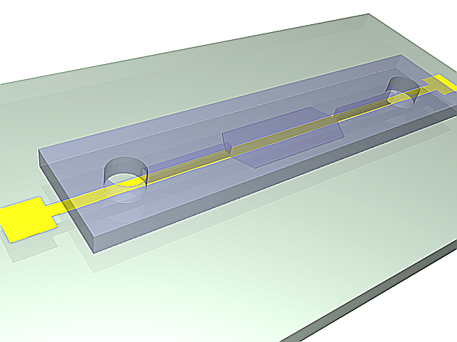

3D model of the molded PDMS chip on a glass substrate (left) and close-up on the entropic trap and the flat center section (right). The yellow line represents the Joule heating element.
Heating elements

To change the temperature of PNIPAM, I designed heating elements using the Joule effect in a resistor, similar to the way a resistor produces heat in a toaster. I created a model to simulate heat transfer, and built the system using semiconductor technologies.
Labs-on-a-chip are interdisciplinary by nature: they involve physical, chemical, and biological effects. A model of a microfluidic system may involve many physical effects to account for all the components integrated into the device.
Multiphysics simulation involves a model with two or more physical phenomena; in my case, Joule heating in the resistor (an electro-thermal effect) and heat transfer through the microfluidic device (a thermal effect). The model might later be expanded to include electrokinetic mixers (microfluidic effects) and biological interaction (sensitive layers).
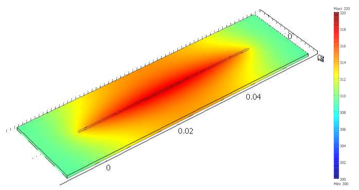
Simulation software like COMSOL Multiphysics is able to model the generation of heat by Joule effect in the resistor, and heat transfer through the glass substrate. However, a 3D model is computationally expensive, particularly when adding the PDMS microchannel on top of the resistor.
The simulation is based on the finite elements method, meaning that we break down the model into a mesh of many small bits, and then approximate the solution in each tiny region. Computers can calculate those estimates numerically, instead of trying to solve partial differential equations analytically in the whole system. The mesh is denser in the main zone of interest.
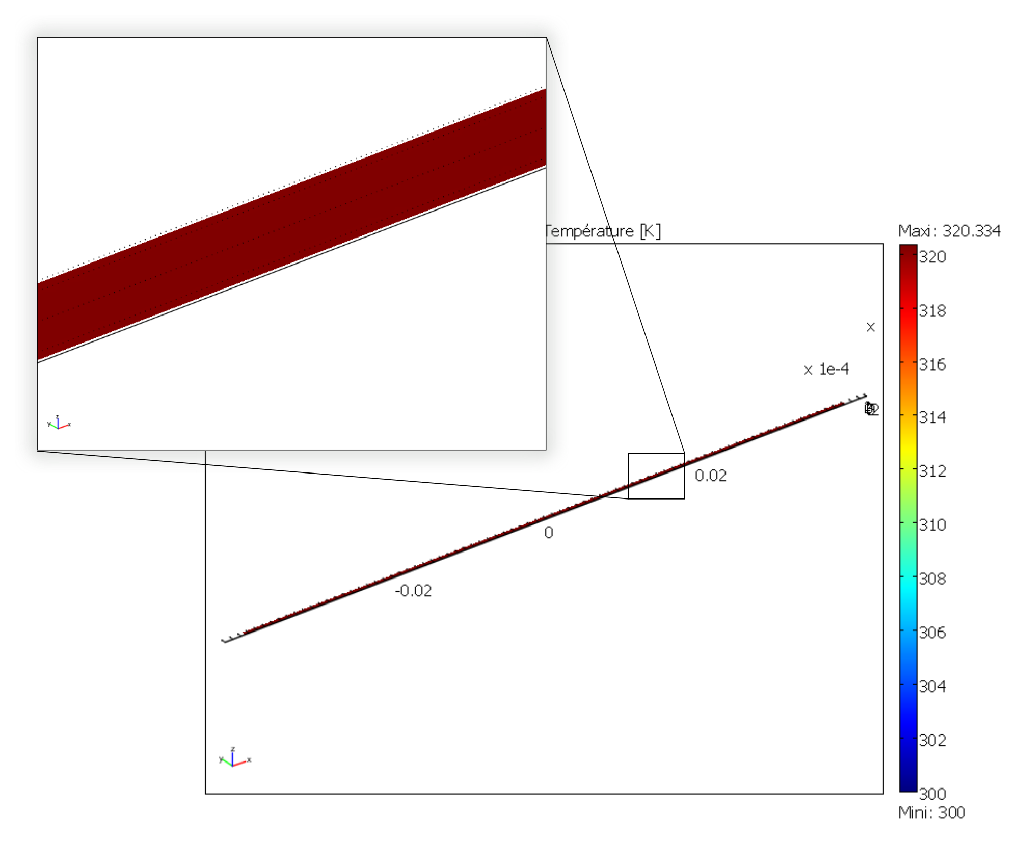
After decoupling the geometry, modeling Joule heating shows a uniform temperature in the gold resistor. The results of this model are then plugged into the heat transfer simulation.
While it’s possible to create one simulation for both phenomena (heat generation and heat transfer), it requires building a complex model for a 3D object with high aspect ratio; computing time can be reduced by simplifying the geometry, and ideally reducing the volume or number of dimensions involved. In other words, the two physical effects are still linked, but solved in two different 2D geometries that are simpler to compute.
Thermal dynamics are driven by the Joule heating that can be solved first. The geometry of the system enables us to solve the heat transfer phenomenon in a 2D cross-section of the channel. The low-ceiling zone of the channel (used to stop the beads from entering) is ignored at first approximation.
Heat transfer is then simulated from the golden resistor to the glass substrate, silica layer, water in the channel, and PDMS structure. Heat convection in the liquid is negligible at this scale, so heat transfer is governed by conduction. The silica layer deposited onto the gold resistor ensures electrical insulation while also providing a surface for functionalization.
The final simulation shows that a simple Joule heating line provides a stable temperature high enough to trigger PNIPAM’s transition in the channel in about 100 ms.
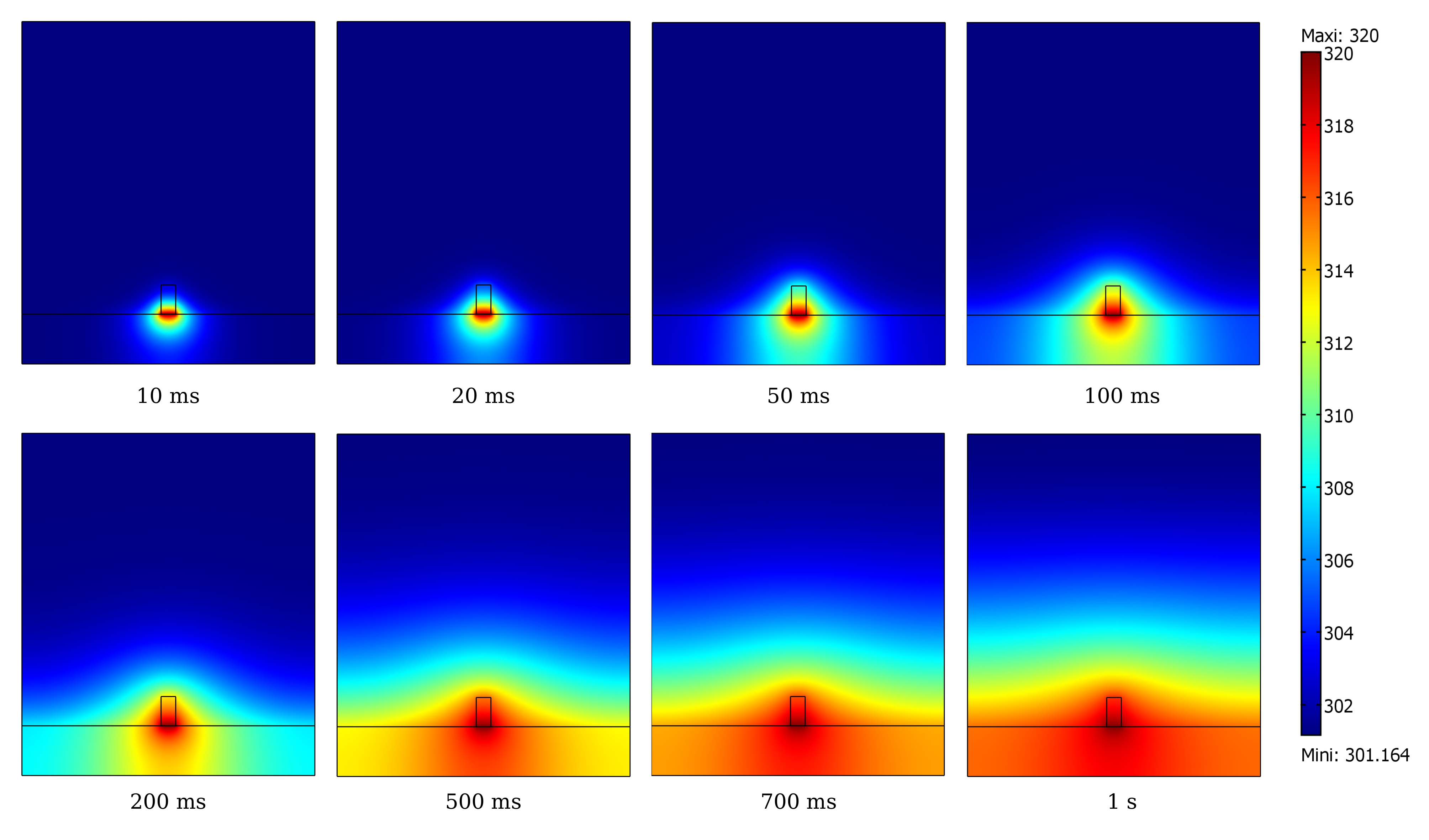
A model of the heat transfer from the Joule resistor into the microfluidic assembly shows that the temperature inside the channel is enough to change the state of PNIPAM within 100 ms (temperature scale in Kelvin).
I built the system using techniques from microelectronics in a clean room environment. The resistor was made by lift-off metal deposition of a 8000 Å gold layer onto a 1000 Å grafting layer of titanium. Polycrystalline silicium, being more resistive than gold, is usually used to create Joule resistors. However, gold deposition is an easier process that the one for polysilicium, which involves low-pressure chemical vapor deposition (LPCVD) at around 600°C. I therefore chose gold for fast-paced, exploratory research.
After building the heating element, I measured the temperature using an infrared camera, and confirmed that it could activate PNIPAM.


Infrared thermography of the Ti-Au Joule resistor shows how it heats up the glass substrate. The resistor itself appears black due to gold’s low emissivity and high reflectivity. The temperature is therefore measured instead on the glass adjacent to the resistor, which is a good approximation in a stationary regime (Top: 0V, 23°C. Bottom: 7 V, 40°C).
Other materials could be investigated to improve the heating element, e.g. polysilicum that would generate heat at lower volage. Gold and polysilicium are both opaque, but there are different ways to maintain transparency for biological applications. For example, indium tin oxide (ITO) is a transparent material that conducts electricity. Another solution is a more elaborate design, based on parallel opaque resistors on each side of the channel.
Catching proteins
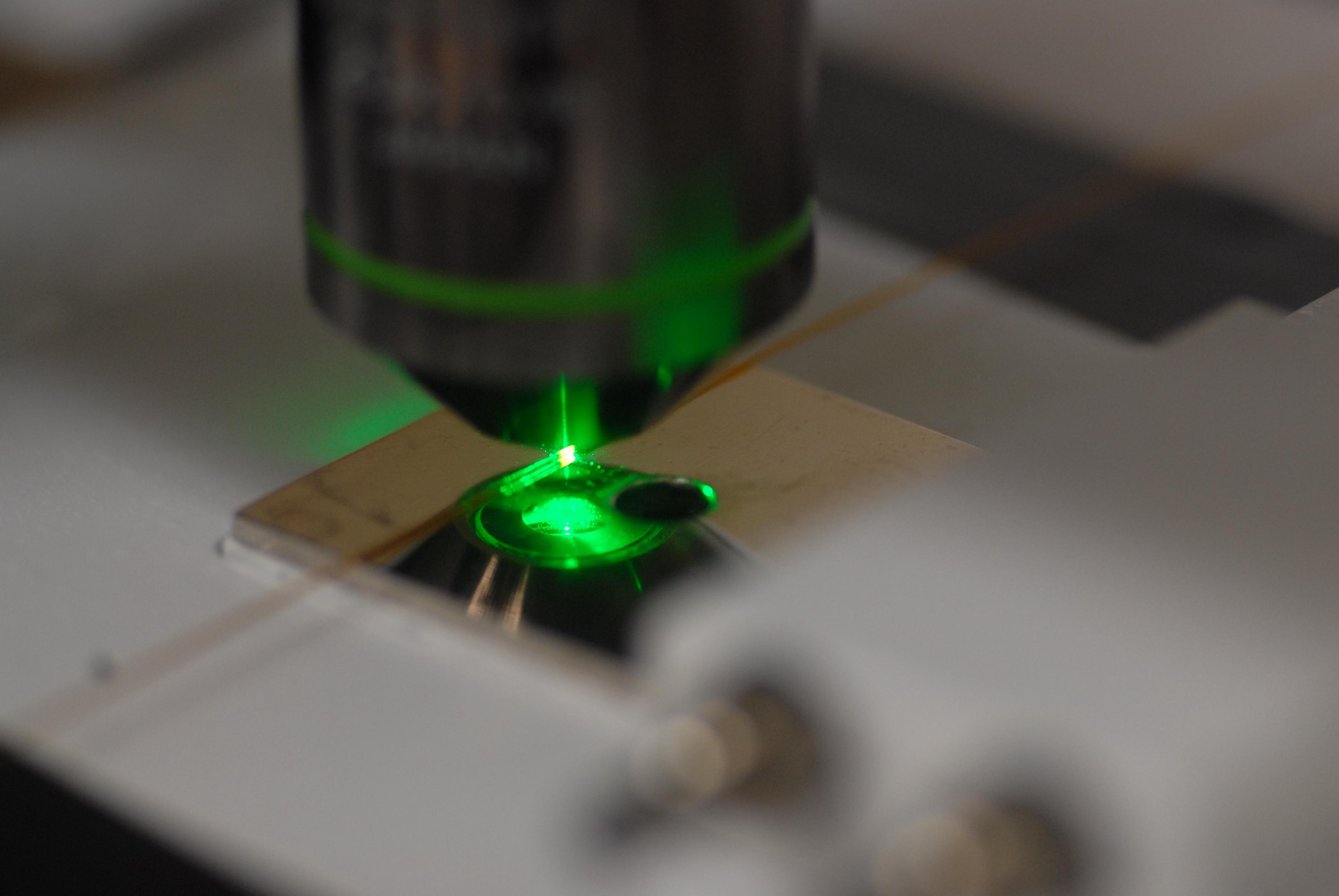
In the last step of my research, I trapped and released proteins on PNIPAM-coated microbeads. I conducted those experiments in capillaries and in the microfluidic chip, and measured the results using fluorescence microscopy.
Labs-on-a-chip aim to provide a remplacement for entire chains of analysis. In particular, micro total analysis systems (µTAS) handle raw samples like blood or urine. Such samples are often mixed with phosphate-buffered saline (PBS), a solution that doesn’t harm most biological molecules of interest. However, the salts present in PBS interfere with some analyses like mass spectrometry, one of the main methods of proteomics (the science of proteins)
Solid-phase extraction consists in trapping biological molecules on solid objects, then releasing them in a cleaner liquid, for example one free of salts. To detach the molecules, scientists often use solvents like acetonitrile, which risk damaging the very biological objects we are trying to detect and analyze.

Biological molecules like proteins stick to PNIPAM in its hydrophobic state, above 32°C. When the temperature drops below PNIPAM’s transition point, the proteins are released. This behavior has applications in the preconcentration of samples in proteomics.
PNIPAM can attach proteins in its hydrophobic (warm) state, and release them in its hydrophilic (cold) state; it can offer a soft chemical layer with a gentler release method, acting as a medium for microextraction.

Proteins and other biological molecules are sometimes present in concentrations too low to be detected: they don’t stand out from background noise (left). Preconcentration consists in trapping molecules and accumulating them (for example on hydrophobic PNIPAM) and then releasing them all together, leading to a cleaner sample and a more visible spike (right).
I coated microscopic silica beads with PNIPAM to use them to trap proteins (a process called adsorption) and release them afterwards (desorption). I conducted those experiments in silica capillaries and in microfluidic chips using fluorescence microscopy: many biological molecules can be combined with a fluorophore, a molecule that absorbs light in one color and re-emits it in another color (at a higher wavelength). Fluorescence can confirm the presence of biological molecules we’re interested in.
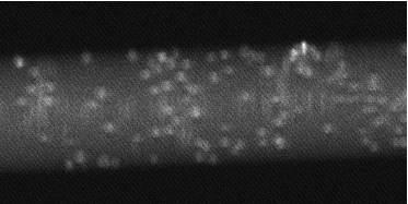
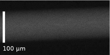
In a silica capillary, silica beads coated with PNIPAM catch albumin–fluorescein isothiocyanate conjugates (left), and release up to 80% of them when the temperature is lowered (right).
Bovine serum albumine (BSA, CAS: 9048-46-8) is often used as a model protein in biology because it is widely available, affordable, stable, and middle-sized (~66 KDa). Florescein (CAS: 2321-07-5, excitation ~495 nm, emission ~521 nm) is a common fluorophore, whose isothiocyanate conjugate (FITC, CAS: 27072-45-3) easily binds to amine groups in proteins. I also conducted experiments with streptavidin conjugated with an Alexa fluorophore.
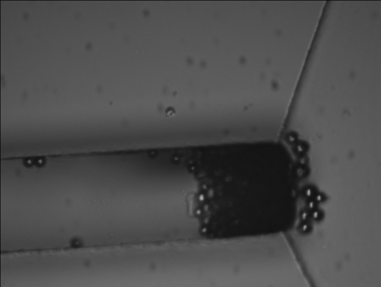
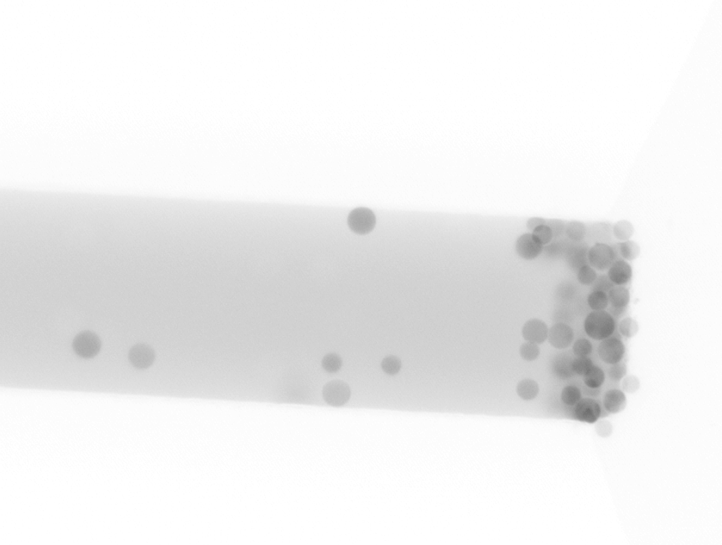
In the microfluidic chip, beads accumulate in the entropic trap before the central section (left, natural light). Fluorescent proteins attach to PNIPAM-coated beads and stand out of the background fluorescence of the solution in the channel (right, inverted fluorescence).
The desorption rate, meaning how much of the proteins detach from the PNIPAM-coated beads, reached 80% in capillaries, but only 60% in the microfluidic chip. The lower rate in the chip is likely due to the beads being packed too densely and not being able to move around. A common technique to control beads in microfluidic systems is to integrate magnetic fields, which can perform functions like actuation, trapping in place, and stirring to help with rinsing. That technology was still under development in my lab at the time.

Alexa-streptavidin conjugates adsorbed on PNIPAM-coated beads and then desorbed up to around 60% when the temperature was lowered.
